
Graham Lab Research Interests(technical): physics of low-dimensional materials and devices, energy flow in condensed phase materials and devices, ultrafast microscopy, decoherence in excitonic systems, light harvesting, interfacial photocurrent generation, novel optical microscopy tool development.
First to get a taste of the type of science we do, why not take a 45s speed-tour of the Micro-Femto Energetics Lab? [Video credit: Kyle T. Vogt, ufE LabPhD Scientist]
We've expanded: Learn about our additonal new Ultrafast Laser Lab Facilities now in full operation. Here we explore microscopy in extreme temperature, time-resolution and magnetics field limits.
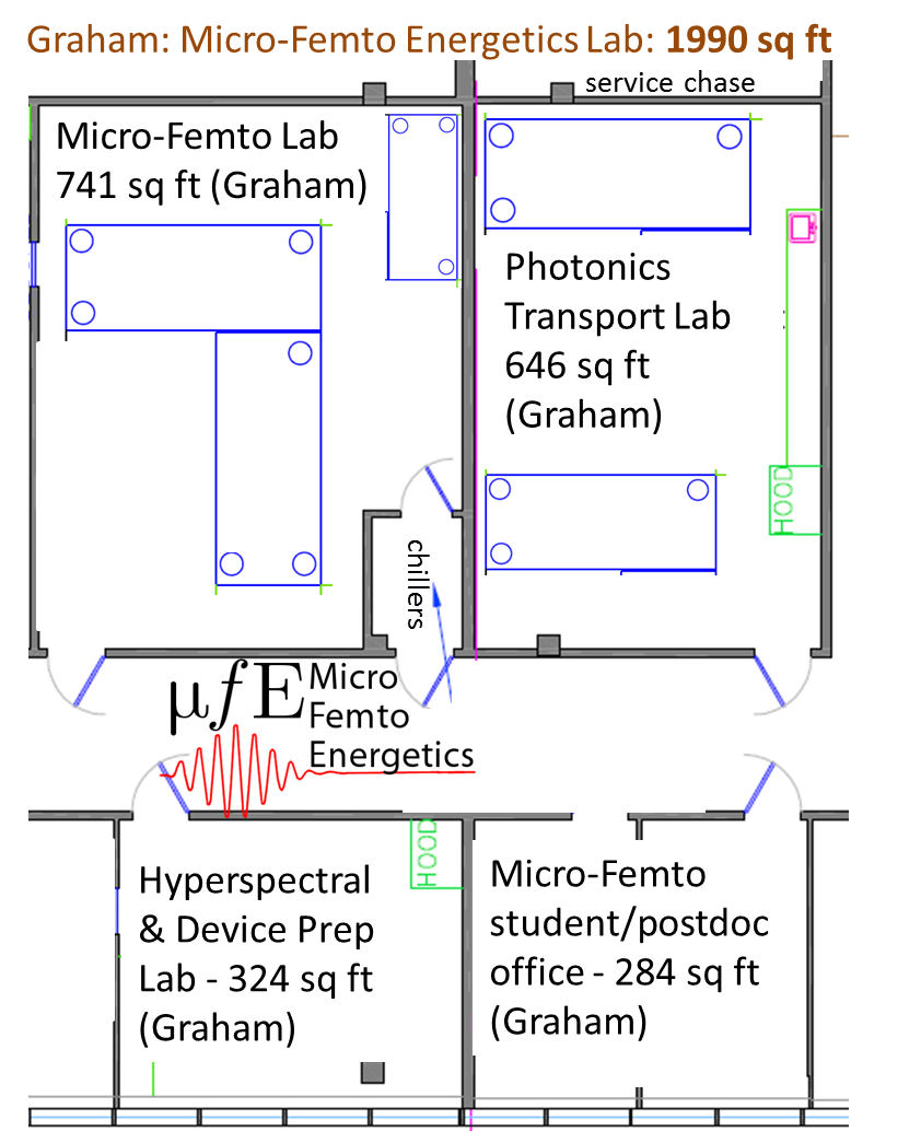
We call our research group the Micro-Femto Energetics Lab. One of our primary goals is to better understand electron flow and relaxation in emerging materials, transistors, solar cells, and other devices. We accomplish this by using tunable short laser pulses to study and "film" electronic excitations across broad spectral (0.1 to 6 eV) and temporal ranges (10 fs to 10 ns). We do this by effectively filming what happens to electrons after they get excited by light. By 'filming' how electrons move and relax in nanomaterials, we find out how to avoid bottlenecks that would ultimately limit the efficiency of a solar cell produced. Since electrons are both very small and move very fast, in order to film electrons new solar cell materials, we require sub-micrometer (<10-6 m) spatial resolution and femtosecond (10-15 s) time resolution. Hence the our lab's name, "the Micro-Femto Energetics Lab" or simply the μ f E Lab.
 How do the physical properties of matter change as materials get small? The μ f E lab is able ‘to film’ the excited electron’s energetic journey from light absorption to photocurrent generation with sub-micron (<10-6 m) spatial resolution and femtosecond (<10-15 s) time-resolution. By 'filming' how electrons move and relax at nanoscale interfaces, we identify the bottlenecks that inherently limit the efficiency of solar voltaics and photosensors.
We investigate energy/current generation and transport at novel material interfaces. With micro-femto precision, we can resolve the electron's journey from initial excitation until current generation. The μ f E Lab will apply these unique measurement tools to a host of emerging materials including 1D/2D nanostructures,organic photovoltaics and biological systems. Our goal is to understand and control the processes drive light, energy and current extraction at nanoscale interfaces. Through this we can intelligently engineer next-generation optoelectronics. transistors and solar voltaics.


