|
RF Design-Course Development |
1 Course description as initially planned
The course will emphasize the experimental laboratory component.
50% of class meetings will be held in the electronics labs in
the form of a studio. The class of 25 students will be divided into four
teams of 6±1 students.
The RF Design course can be best described by the following scenario:
For the first class meeting, four cardboard boxes will be brought to
class, each containing various electronic modules. There will be one box
for each team to use during the semester.
Each box contains about 30 modules which (if connected together)
function as a Gigaherz-range transmitter/receiver (two-way radio). Each
team member is given 5 modules for the duration of the semester. The
modules are labeled and specified such that it is clear what kind of
function they perform. However, the details of their design are unknown
(the board can be painted over to hide the layout).
The goal of each student will be to design and build the equivalents of
the five modules. Each student is individually responsible for
designing and building his modules. But also, the modules are parts of
the entire communications system. The whole team must work together on
the entire system to clarify the input/output dependencies between the
modules. The grade for each student will depend both on the individual
work and collaborative work in certain percentages (to be established).
The main advantage of the proposed approach to teaching the RF design is
that from the beginning of the semester each team has a working radio to
experiment with. Students can learn about individual modules, measure
them and draw conclusions from the live hardware. It will be up to the
students to decide what kind of knowledge they need to learn to be able
to design and build the modules. After the semester is over, the
students will have five circuits each to present to their prospective
employers during the job interview.
2 Participants
A group of people is involved in developing the RF Design class:
(send group email)
3 Weekly meetings
1/12/2004
Fist, we talked about the structure of the system that we are going to
build. There will be two antennas made of cans, and there will be two
circuits; one for transmitter and one for receiver. The system will
work at 2.4GHz frequency. Pringles cans are suitable for this frequency.
The bandwidth will be around 100 MHz, suitable for the standard Ethernet
signal.
There will be modules like filters, VCO's and frequency converters in
the transmitter and receiver. Transmitter circuit will have to deliver
enough power for the receiver in given conditions.
There will be around 30 modules in two circuits. Everyone in the group
will be responsible for 5 of them. Everyone should build one module
every three week. PCB will be used for building every module. We might
use a chemistry lab because there will be lots of etching. The circuit
will be made up from PCB boards connected to each other directly or by
coaxial cables. We are planning to put the modules chip enclosures.
Before the modules are built, we will use function generator and
spectrum analyzer to find out the gain and noise properties of the
antennas.
The RA will be responsible for learning how to use the equipment. All
the materials and manuals will be given to the RA, and they will be
posted on web. All the meeting reports will be posted on web.
There will be meetings on Mondays from 04:30p to 05:30p
On the next meeting:
The way to build the inductance, which will be used in VCO, will be
ready. What to do first and next will be discussed. The properties of
the antennas will be discussed. So that some of the properties of the
modules will be found.
1/19/2004
Andy will work on selecting the oscillator circuit for the VCO.
Steve will use the inside of an old HP sweeping generator to produce an
AM modulated signal in the GHZ range. Ultimately this will become a
project on the AM modulator for the transceiver.
Open question: how much power do we need in the transmitting antenna to
be able to go through two leyers of standard shingles of a typical
house. This would enable placing the system at the attics.
1/26/2004
Alper figured out how to properly calibrate the network analyzer. It
turns out that the improvised terminations and vias are sufficient to
calibrate the analyzer - no Agilent kit will be necessary. The overall
goal is to build things cheaply and from scratch.
Sasi will review approaches to build the amplifier with
impedance-matched input and output. Several stages of such amplifier
will be used in various places in the transceiver circuit.
Dave is studying Ansoft simulators to master such skills and create some
documentation on the software use for future students to use. Ansoft
Designer has too many features disabled in the student version to be
really useful. We will go with Serenade which has the harmonic balance
enabled.
We bought some parts:
Quantity  Digikey code

20        BFP405INCT-ND     RF transistor, case SOT-343, price 0.5800

20        NE85634CT-ND      RF transistor, case SOT-89, price 0.9000

16        MA2S37700LCT-ND   varicap diode, case SS-mini, price 0.4400

10        MA2SV0200LCT-ND   varicap diode, case SS-mini, price 0.4300
2/02/2004
While waiting for the parts to come, Andy used the 2N 5770 to construct
an oscillator and maximize the frequency of oscillations. The result is
shown in Fig. 1. Not bad at all for the breadbord! The
actual design should be easier, since the BFT405 has ft=25GHz.
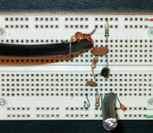
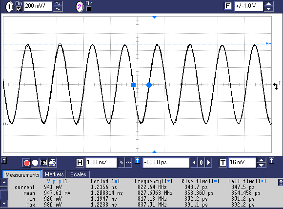 Figure 1: A 827MHz Hartley oscillator built using a transistor with
fT=1GHz in the common-base topology. The shorted stub functions
an inductor for the tank circuit in the emitter. Two turns of a
resistor lead makes up the base inductor.
Figure 1: A 827MHz Hartley oscillator built using a transistor with
fT=1GHz in the common-base topology. The shorted stub functions
an inductor for the tank circuit in the emitter. Two turns of a
resistor lead makes up the base inductor.
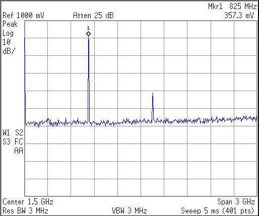
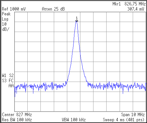 Figure 2: The spectrum of the 827MHz oscillator.
Sasi has preliminary design consideration on how to build the amplifier
for 50Ohm input and output and 2.4GHz.
Figure 2: The spectrum of the 827MHz oscillator.
Sasi has preliminary design consideration on how to build the amplifier
for 50Ohm input and output and 2.4GHz.
2/10/2004
We discovered that Pringle cans are coated with some plastic on the
inside so that the connector does not stick to it very well. Moreover
the sheet resistance of the metal foil used on the inside of the cans is
quite high. We decided to go with coffee cans instead, shown in
Fig. 3.
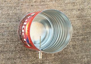
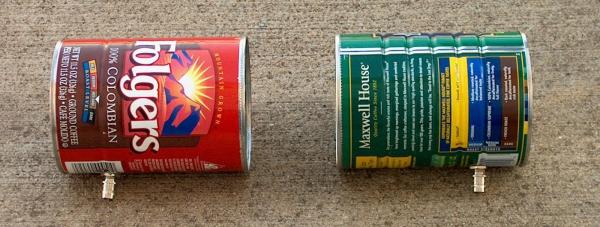 Figure 3: Coffee can antennas.
Alper made some initial measurements on the coffee can antenna with
the N-type connector made by Dustin.
Figure 3: Coffee can antennas.
Alper made some initial measurements on the coffee can antenna with
the N-type connector made by Dustin.
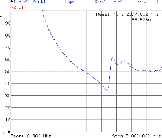 Figure 4: The coffee can antenna impedance sweep Z(f).
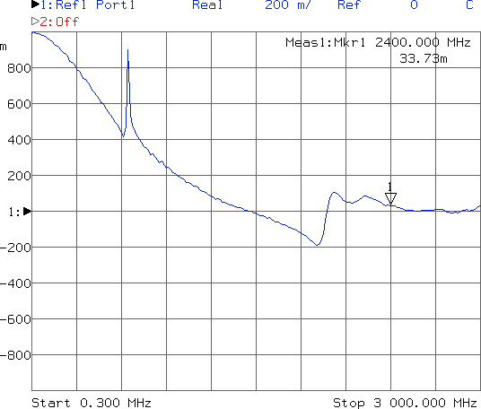
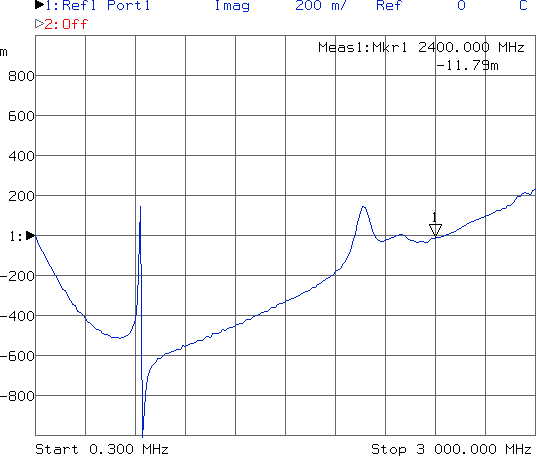 Figure 5: The coffee can antenna. Resistance R(f) (left) and reactance
X(f) (right) sweeps.
More measurements will be made and compared with additional can antennas
produced with the panel-mount BNC connectors.
The VCO is finally working! The circuit is primarily the Colpitts
oscillator. It is build on a copper board with the microstrip inductor
and SMD transistor BFP 405, SMD varactors MA2S377, and SMD
capacitors, the rest of the parts are regular feed-through. The output
is only weakly connected to the tank circuit through 20dB
coupling. This makes the output very low, but the stability of the
oscillator is not compromised by the load.
Figure 5: The coffee can antenna. Resistance R(f) (left) and reactance
X(f) (right) sweeps.
More measurements will be made and compared with additional can antennas
produced with the panel-mount BNC connectors.
The VCO is finally working! The circuit is primarily the Colpitts
oscillator. It is build on a copper board with the microstrip inductor
and SMD transistor BFP 405, SMD varactors MA2S377, and SMD
capacitors, the rest of the parts are regular feed-through. The output
is only weakly connected to the tank circuit through 20dB
coupling. This makes the output very low, but the stability of the
oscillator is not compromised by the load.
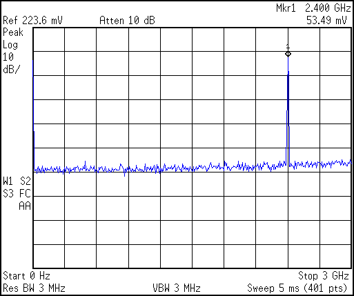
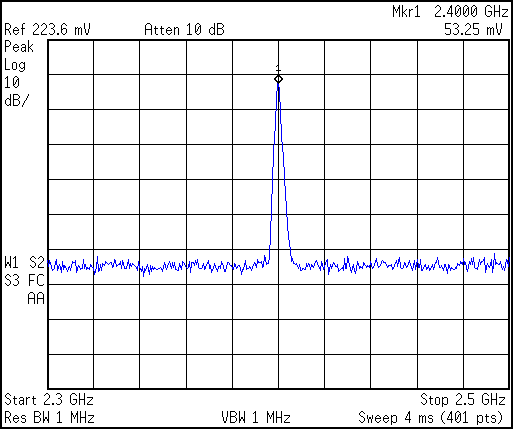 Figure 6: Spectrum of the 2.4GHz VCO.
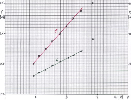 Figure 7: Characteristic of the VCO.
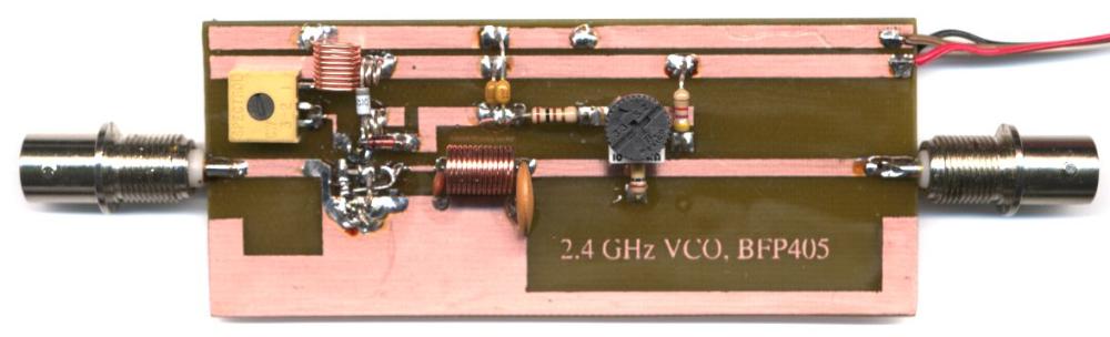 Figure 8: The VCO.
Enclosure from Lowes:
"Handy Box Welded", $1.07, Model #8650, Item #19849
Made by Hubbel Electrical Products and Raco
Dimensions 4"×2"×1[1/2]" deep.
Figure 8: The VCO.
Enclosure from Lowes:
"Handy Box Welded", $1.07, Model #8650, Item #19849
Made by Hubbel Electrical Products and Raco
Dimensions 4"×2"×1[1/2]" deep.
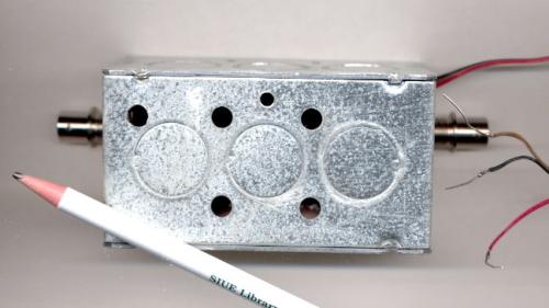
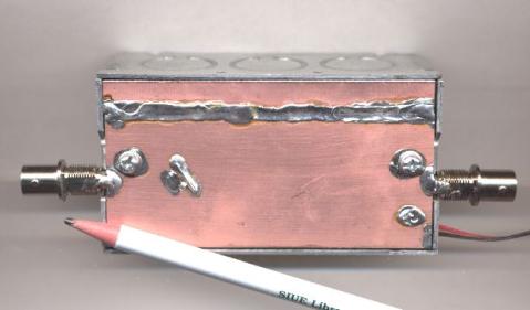 Figure 9: The VCO enclosed in the metal box.
3/1/2004
Alper experimented more with can antennas. He was trying to determine if
there is an advantage of a longer antena over the shorter one. In
particular if a long antenna is more directional. There was no
signifficant improvement in the beam shape over the distance from one
work station to the other in the Electronics Lab. Therefore, for now we
will go with coffee cans then. They are easier to build than the long
antenna, shown in Fig. 10.
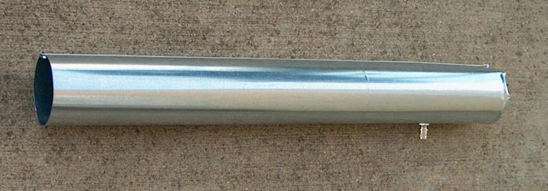 Figure 10: Long antenna made from sheet metal.
3/15/2004
We discussed various approaches to up- and downconvert the signal. The
final decission will be based on the properties of the signal to be
transmmitted. We plan on sending the standard 100bit/s Ethernet
signal. We were concerned if the DC is a necessary component of the
signal and how much of the low frequency component is required for
errorless operation of network cards.
To investigate the baseband signal, Steve created a breakout box out of
an Ethernet hub. Each socket contains two twisted-pairs: the
transmitting pair TX and the receiveing pair RX. There are a few of the
sockets for clients and one socket for host (numbered as 1). Steve
tapped into two of these sockets to get the signals out of the
enclosure. We used standard coax cables to interconnect the TX-RX pairs
keeping the hub disconnected from its power supply. Also, we used a
capacitor to remove the DC from one of the signal paths. The lowest
capacitance value still enabling errorless Ethernet transmission was
10nF.
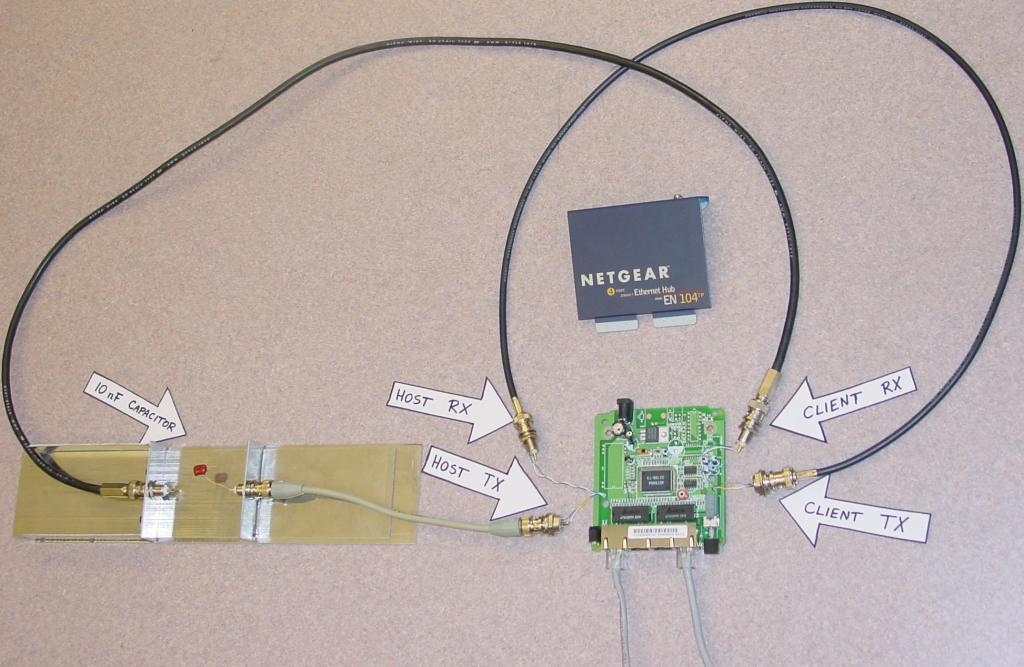 Figure 11: Ethernet hub made into a break-out box for testing signals.
None of the wires in the twisted pairs cannot be grounded. This means
that we will have to convert from differential to asymmetric signal
before we use it in further stages. For now the breaout box will be
modified to have four BNC connectors for host and four BNC connectors
for client - each wire spearately. We tested that as well.
Figure 11: Ethernet hub made into a break-out box for testing signals.
None of the wires in the twisted pairs cannot be grounded. This means
that we will have to convert from differential to asymmetric signal
before we use it in further stages. For now the breaout box will be
modified to have four BNC connectors for host and four BNC connectors
for client - each wire spearately. We tested that as well.
3/29/2004
We are ready to build the high-gain amplifier for the carrier signal
produced by the VCO. The design is a cascode of common-base and
common-collector stages. Out of the three possible combinations, this
selection seemed to be the most stable and the closest to the optimal
impedance match. The BFP 405 transistors are used. We can count on at
least 20dB gain at 2.4GHz frequency.
The circuit is fabricated using the product called Press-n-Peel PCB
Transfer Film. First, the circuit layout needs to be designed such that
it can be printed with exact geometries as specified by calculations and
simulations. We use 98mm × 50mm size board, because
it nicely fits in the metal enclosure. The raw double-sided copper board
has to be cut to size, as shown in Fig. 12. Using Brillo
pads, the board needs to be nicely cleaned on both sides so that the
copper surface has no evidence of fatty residum comming from our
fingers.
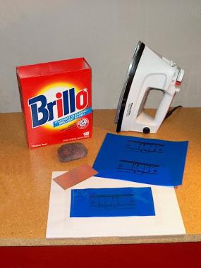
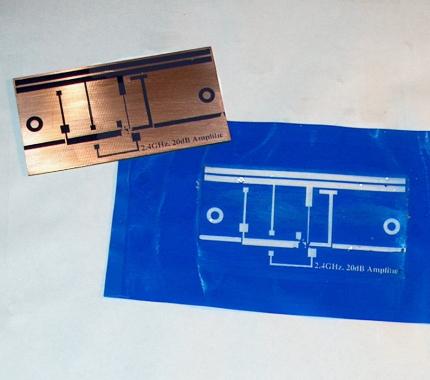
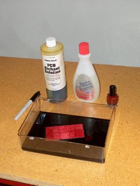 Figure 12: Fabrication of a double-sided printed circuit board
(PCB). Cleaning and layout transfering (left), transferred layout
(middle), etching (right).
The layout should be printed in reverse (mirror image) on the
Press-n-Peel blue sheet. It is a good idea to print multiple copies of the
layout on the same sheet in case we have to redo the process. As shown
in Fig. 12, one copy of the layout is cut from the sheet, the
copper board placed underneth it and everything is fixed together with
scotch tape.
The printer toner will transfer from the blue sheet to the copper board
when heated with the iron. Refering to the Press-n-Peel manual, the iron
should be set between acrylic and polyester setting. It takes less then
5 minutes of ironing to warm up the board so that the toner fully
detaches from the blue sheet. Unfortunately there is no way to tell when
the board is ready. After the heating time, the board and the sheet are
stuck together. The board can be cooled down under the cold water. The
sheet should be peeled off the board, as shown in
Fig. 12. There will be places with missing toner. Small
problems can be fixed with a permanent marker. Bigger missing patches
can be covered with the regular nail polish.
In case there are too many problems, it is generally better to start
over on the other side of the board. The iron temperature can be
readjusted according to the type of problem. If too hot, the toner melts
completely and distorts the layout. If too cold, the toner does not
transfer completely. It is a good idea to mark the optimum iron setting
for the future times.
When the transfered layout is in a satisfactory condition, the other
side of the board should be fully covered with the nail polish. The
other side will serve as a ground plane for microstrips. On the front
side, the unmasked copper will be etched out from the board in the
etching solution. In the figure, ferric chloride solution is used. If
the board is dropped flat on the solution surface it will float. This
promotes etching since there is no sediment settling on the board. Be
aware that ferric chloride permanently stains clothing. About twenty
minutes of time is sufficient to finish etching. The board should then be
washed in water and the nail polish and the toner should be removed with
the nail polish remover. The leftover toner can be further removed with
the Brillo pad.
Figure 12: Fabrication of a double-sided printed circuit board
(PCB). Cleaning and layout transfering (left), transferred layout
(middle), etching (right).
The layout should be printed in reverse (mirror image) on the
Press-n-Peel blue sheet. It is a good idea to print multiple copies of the
layout on the same sheet in case we have to redo the process. As shown
in Fig. 12, one copy of the layout is cut from the sheet, the
copper board placed underneth it and everything is fixed together with
scotch tape.
The printer toner will transfer from the blue sheet to the copper board
when heated with the iron. Refering to the Press-n-Peel manual, the iron
should be set between acrylic and polyester setting. It takes less then
5 minutes of ironing to warm up the board so that the toner fully
detaches from the blue sheet. Unfortunately there is no way to tell when
the board is ready. After the heating time, the board and the sheet are
stuck together. The board can be cooled down under the cold water. The
sheet should be peeled off the board, as shown in
Fig. 12. There will be places with missing toner. Small
problems can be fixed with a permanent marker. Bigger missing patches
can be covered with the regular nail polish.
In case there are too many problems, it is generally better to start
over on the other side of the board. The iron temperature can be
readjusted according to the type of problem. If too hot, the toner melts
completely and distorts the layout. If too cold, the toner does not
transfer completely. It is a good idea to mark the optimum iron setting
for the future times.
When the transfered layout is in a satisfactory condition, the other
side of the board should be fully covered with the nail polish. The
other side will serve as a ground plane for microstrips. On the front
side, the unmasked copper will be etched out from the board in the
etching solution. In the figure, ferric chloride solution is used. If
the board is dropped flat on the solution surface it will float. This
promotes etching since there is no sediment settling on the board. Be
aware that ferric chloride permanently stains clothing. About twenty
minutes of time is sufficient to finish etching. The board should then be
washed in water and the nail polish and the toner should be removed with
the nail polish remover. The leftover toner can be further removed with
the Brillo pad.
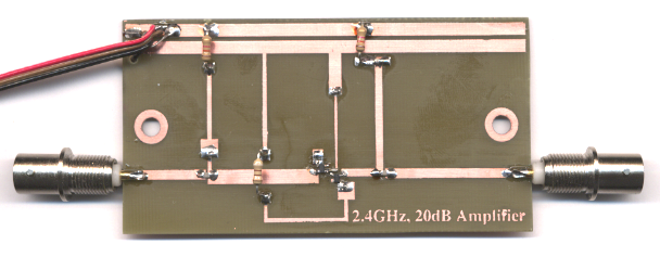 Figure 13: The amplifier.
4 Strategy changes
4.1 Photo-litographic PCB development
After sever trials it became evident that the Press-n-Peel technology
does not provide enough accuracy on fine details of the PCB layout. It
is practically impossible to accomplish a good quality trace of the
width less than 0.5mm. A frequency mixer circuit has been
built. Fine trace separations between coupled lines could not be
accomplished. This resulted in unacceptable power loss beyond 40dB.
The team decided to abandon the Press-n-Peel approach and find a
simple way to arrange a photo-litographic PCB development
process. Ultra-violet exposure box and positive photo-resist substrate
material has been acquired to make new boards. Previously quite thick
boards were used. The decission was made to go with much thinner
boards. Most of the insertion loss in the circuits will be due to the
cheap FR4 dielectric material, not the copper resistivity. Therefore it
was reasonable to reduce the dielectric width trading it for the reduced
trace width. The new choice was the Injectorall 30mil board with 1 oz
copper. Thinner boards would be to fragile and easily break when dragged
across the table by the cables.
4.2 RF simulator: Ansoft Designer
It has been near impossible to effectively design RF circuits from
equations. Secondary effects are to signifficant to ignore in the
process of prototyping. There is no practical way to account for such
secondary effects without careful simulation. Initially, to avoid
problems, certain methods of circuit design were used such us placing
grounding capacitors inside a whole drilled through the board, or
placing the ground plane on the trace layer of the board. However, the
design process and circuit fabrication are tedious and
counter-productive. They are also questionable from the educational
perspective.
With the help of the School of Engineering Computer Committee who
provided funds, and Ansoft Corporation which offered tremendous
educational discount, the state-of-the art simpuation software Ansoft
Designer was acquired and installed in the lab computers. Now we have
access to the same resource the industry is currently using. This took
us out of a few-month long stagnation.
4.3 Course format change
It became evident that the initial plan of 30 modules to build is
infeasible. The format for the course will be changed keeping the main
objectives intact. They are:
- The course emphasizes the laboratory experience.
- After completing the course, every student has built a few nontrivial
RF circuits.
Throughout the semester, every student will build three circuits: an
amplifier, a VCO, and a mixer. In the VCO, the amplifier circuit will be
incorporated. In the mixer, the VCO and the amplifier circuit will be
incorporated. This way tha final circuit will become a complete
2.4GHz tuner, and the design consists of three incremental steps.
File translated from
TEX
by
TTH,
version 3.61.
On 28 Sep 2004, 11:18.